Flying Probe Test (FPT) – PCB Assemblies Flying Probe Test Guidelines
By: Admin November 14, 2019


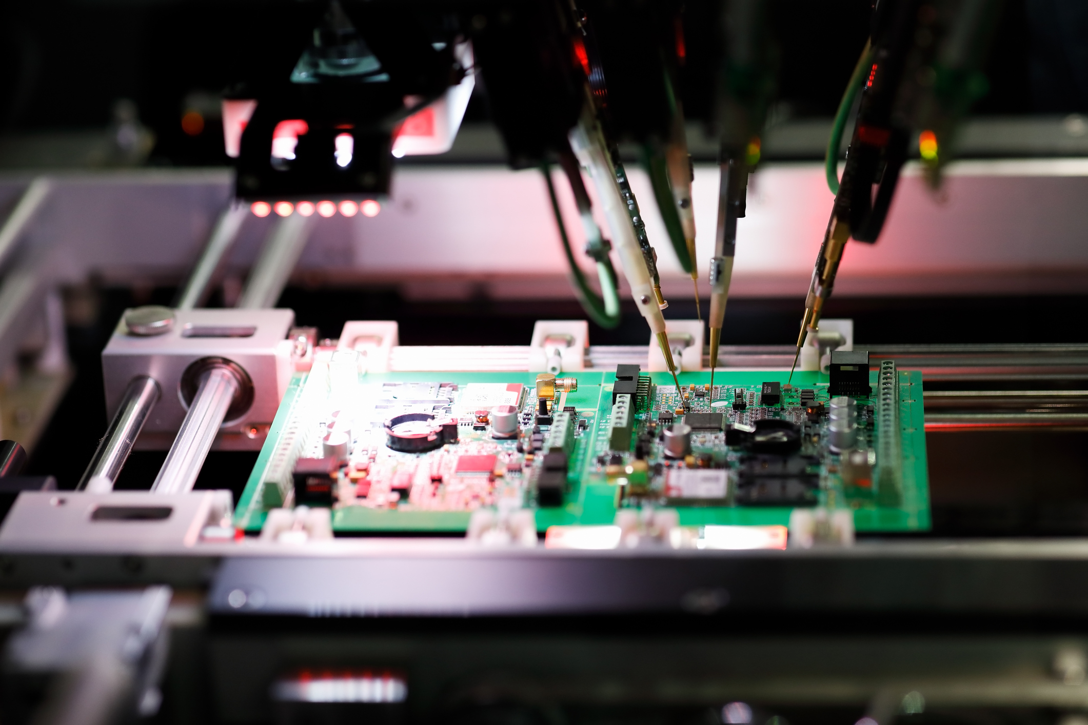
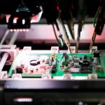
Over the last few years, flying probe test have become an increasingly popular test method, in comparison to traditional PCBA in-circuit tests, due to less stringent design requirements and the elimination of high fixturing and programming costs.
Flying probe testing doesn’t require a dedicated testing fixture and can easily adapt to different PCBA layouts and designs through programming, making flying probe testing a cost-effect in-circuit solution for low to medium volume, as well as, prototype assemblies.
While flying probe test can easily adapt to various PCBA prototype layouts and designs, a focus on the following PCBA components will increase test accuracy and decrease the risk of board damage:
Board Rail
A border edge on opposite sides and at least 6mm wide (free of components) should available to allow for placement in the machine. This border edge can be panel waste or space included in the design.
Fiducials
A minimum of 3 fiducials (2 diagonal) should be available as reference points for the machine to diagnose probe placement. These can be composed of panel waste or be incorporated into the PCB cast (recommended).
Vias
If probing the edge of PCB vias, vias must NOT be tented. It is recommended to include the “non-tented” specification in your PCB design.
Component Legs
Dedicated space is critical when probing near component legs. It is recommended to leave space near the “toe” of component legs to have a good solder joint and never probe directly on the component legs.
Probe Points
Ground and power rail probe points should be easily accessible. The bottom side of the PCB is recommended. Easily accessible probe points can reduce the time and costs associated with flying probe testing.
Test Access
If using a single-sided machine, designate at least one side of the assembly to testing by allowing at least one point for each network to be easily accessible to the probe.
Component Height
Component height on both sides of the assembly, should be approximately 40mm-90mm. Components with heights exceeding maximum height can create a “No Fly” zone that can inhibit accessibility to the assembly.
Size
Test access points should be close together to decrease the time it takes for a probe to move between measurement points; especially if the assembly is large.
Flying probe testing has many advantages compared to traditional “bed of nails” testing, with the exception of time. Flying probe testing is slower than other testing methods, which is why it is important to find an experienced EMS provider that Designs for Manufacturability and follows Flying Probe Testing guidelines and best practices.
Flying probe testing is one of many steps in Fit PCB’s test-and-burn in process used to minimize PCB failure and support product longevity.
For additional information about Green Test-and-Burn In services, or other services required for your next project, contact Fit PCB today.